| CPC H03K 5/15006 (2013.01) [H03K 5/131 (2013.01); H03K 19/096 (2013.01)] | 10 Claims |

|
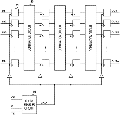
1. A clock enabler circuit, comprising:
a state holding unit configured to perform, based on an internal clock signal, a holding operation of a state, wherein the state indicates whether to output an output clock signal;
a clock signal output unit configured to control the output of the output clock signal based on the state held in the state holding unit; and
a control unit configured to:
receive a clock signal and a clock enable signal from an outside of the control unit; and
supply, to the state holding unit, the internal clock signal and a value of the state that are for the holding operation, wherein
the supply is based on the clock signal and the clock enable signal, and
the state holding unit includes a delay unit configured to delay a timing at which the value of the state is supplied to the state holding unit.
|