| CPC H03K 17/6872 (2013.01) [H03K 19/018521 (2013.01); H03K 19/20 (2013.01)] | 11 Claims |

|
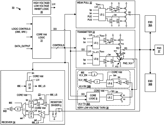
1. A general-purpose input/output (GPIO) apparatus of a system on chip (SoC) comprising:
a first transmitter adapted in response to one or more first gating control signals to supply transmit data to an input/output (I/O) pad in response to output data generated by a low voltage core logic operating within a functional specification voltage range for data transmit operations, the first transmitter comprising an output stage connected to the I/O pad;
a first receiver adapted in response to one or more second gating control signals to supply receive data to the low voltage core logic operating within the functional specification voltage range in response to input data received at the I/O pad for data receive operations;
a first very low voltage transmitter adapted in response to one or more third gating control signals to supply low voltage transmit data to the output stage of the first transmitter and not directly to the I/O pad in response to output test data generated by the low voltage core logic operating with a very low core supply voltage; and
a first very low voltage receiver adapted in response to one or more fourth gating control signals to supply very low voltage receive data to the low voltage core logic operating with the very low core supply voltage in response to input data received from the output stage of the first transmitter and not directly from the I/O pad.
|