| CPC H01S 5/4018 (2013.01) [G01R 31/2601 (2013.01); G01R 31/2635 (2013.01); G01R 31/44 (2013.01); H01S 5/0014 (2013.01); H01S 5/0087 (2021.01); H01S 5/02255 (2021.01); H01S 5/02257 (2021.01); H01S 5/0237 (2021.01); H01S 5/3013 (2013.01); H01S 5/005 (2013.01); H01S 5/0071 (2013.01); H01S 5/02208 (2013.01); H01S 5/02325 (2021.01); H01S 5/02345 (2021.01); H01S 5/4031 (2013.01)] | 19 Claims |

|
1. A light emitting device comprising:
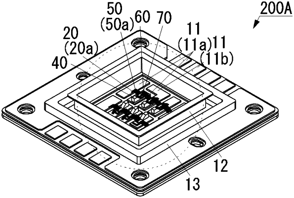
a base comprising a first wiring, a second wiring, and a third wiring;
a first semiconductor laser element electrically connected to the first wiring and the second wiring, at an upper surface side of the base; and
a second semiconductor laser element electrically connected to the second wiring and the third wiring, at the upper surface side of the base; wherein:
the base comprises a frame surrounding the first semiconductor laser element and the second semiconductor laser element in a top view;
the light emitting device further comprises a base cap fixed to the frame such that the first semiconductor laser element and the second semiconductor laser element are enclosed in a space defined by the base and the base cap;
the first semiconductor laser element and the second semiconductor laser element are connected in series;
a portion of the first wiring, a portion of the second wiring, and a portion of the third wiring are exposed at locations outside the space defined by the base and the base cap;
the first wiring comprises a first part that is located inside the space defined by the base and the base cap, and a second part that is exposed at a location outside the space defined by the base and the base cap;
the first wiring, the second wiring, the first semiconductor laser element and the second semiconductor laser element are connected in series;
the second wiring, the third wiring and the second semiconductor laser element are connected in series; and
the second wiring, the third wiring and the first semiconductor laser element are not connected in series.
|