| CPC H01S 5/2275 (2013.01) [H01L 33/06 (2013.01); H01L 33/08 (2013.01); H01L 33/10 (2013.01); H01L 33/32 (2013.01); H01L 33/382 (2013.01); H01L 33/387 (2013.01); H01L 33/44 (2013.01); H01S 5/0655 (2013.01); H01S 5/1064 (2013.01); H01S 5/2004 (2013.01); H01S 5/32341 (2013.01); H01L 33/105 (2013.01); H01L 33/20 (2013.01); H01L 33/28 (2013.01); H01L 2933/0016 (2013.01); H01L 2933/0066 (2013.01); H01S 5/183 (2013.01); H01S 5/34333 (2013.01)] | 30 Claims |

|
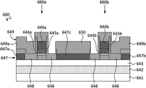
1. A light emitting device comprising:
a first active layer on a substrate, at least a first portion of the first active layer comprising a first electrical polarity;
a current spreading length; and
a plurality of mesa regions on the first active layer, wherein each mesa region comprises:
at least a second portion of the first active layer;
a light emitting region on the second portion of the first active layer, the light emitting region having a thickness and being configured to emit light, the emitted light having a target wavelength from 200 nm to 300 nm, the light emitting region having a dimension parallel to the substrate smaller than twice the current spreading length; and
a second active layer on the light emitting region, at least a portion of the second active layer comprising a second electrical polarity,
wherein one or more of the first active layer, the light emitting region, or the second active layer comprises ZnO, MgO, or BN.
|