| CPC H01S 5/227 (2013.01) [H01S 5/02315 (2021.01); H01S 5/02345 (2021.01); H01S 5/0239 (2021.01); H01S 5/0265 (2013.01); H01S 5/04256 (2019.08); H01S 5/12 (2013.01); H01S 5/2224 (2013.01); H01S 2301/176 (2013.01)] | 20 Claims |

|
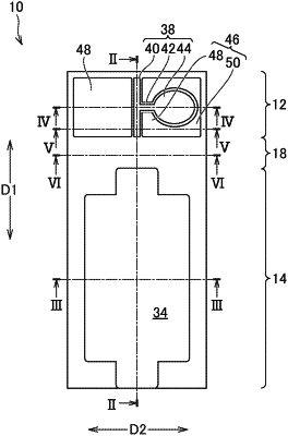
1. An optical semiconductor device comprising:
a semiconductor substrate with a protrusion,
wherein the protrusion forms a lower end portion of a mesa stripe structure in a stripe shape extending in a first direction along an optical axis;
a multi-quantum well layer in a stripe shape extending in the first direction on the protrusion,
wherein the multi-quantum well layer forms an intermediate portion of the mesa stripe structure;
a semiconductor layer in a stripe shape extending in the first direction on the intermediate portion,
wherein the semiconductor layer forms an upper end portion of the mesa stripe structure;
a semi-insulating semiconductor layer in contact with side surfaces of the mesa stripe structure on both sides in a second direction perpendicular to the first direction;
a first electrode on a surface, opposite the protrusion, of the semiconductor substrate;
a second electrode including a mesa electrode on the upper end portion of the mesa stripe structure,
wherein the second electrode includes a lead-out electrode extending in the second direction from the mesa electrode,
wherein the second electrode includes a pad electrode connected to the lead-out electrode; and
a metal film including a first portion positioned on both sides of the lead-out electrode in the first direction and on an upper surface of the semiconductor substrate next to the protrusion in the second direction and not covered by the semi-insulating semiconductor layer,
wherein the first portion is positioned adjacent to the lead-out electrode and between the pad electrode and the mesa electrode, and
wherein the metal film includes a second portion positioned next to and not contacting the pad electrode and continuously integrated with at least part of the first portion.
|