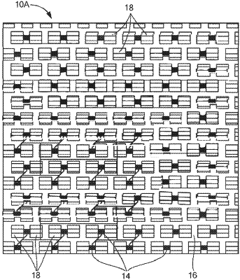
| CPC H01Q 3/34 (2013.01) [H01Q 1/2283 (2013.01); H01Q 21/06 (2013.01); H01Q 21/245 (2013.01)] | 20 Claims |

|
1. A phased array system comprising:
a substrate;
a plurality of elements on the substrate;
first and second beamforming ICs on the substrate, each beamforming IC having a first and second element interface sets configured to be polarized in two different polarizations, a first common interface electrically coupled with the first set of element interfaces, and a second common interface electrically coupled with the second set of element interfaces;
a first interconnect element electrically coupling the first common interface of the first beamforming IC with the second common interface of the second beamforming IC; and
a second interconnect element electrically coupling the second common interface of the first beamforming IC with the first common interface of the second beamforming IC without the second interconnect element crossing over the first interconnect element.
|