| CPC H01L 33/62 (2013.01) [H01L 25/0753 (2013.01); H01L 25/167 (2013.01); H01L 27/1214 (2013.01); H01L 33/06 (2013.01); H01L 33/32 (2013.01); H01L 33/505 (2013.01); H01L 33/54 (2013.01); H01L 33/60 (2013.01); H01L 23/3185 (2013.01); H01L 33/486 (2013.01); H01L 33/507 (2013.01)] | 5 Claims |

|
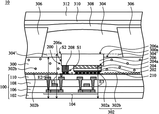
1. An electronic device, comprising:
a substrate;
a driving circuit disposed on the substrate;
a diode electrically connected to the driving circuit;
a light shielding element overlapping the substrate;
a protective layer disposed on the substrate; and
a wavelength conversion layer overlapping the diode,
wherein a surface of the light shielding element has a first width, a horizontal cross-section of a portion of the light shielding element has a second width, the second width is greater than the first width in a cross-sectional view, and the surface is closer to the substrate than the horizontal cross-section of the portion, and
wherein the wavelength conversion layer and the protective layer respectively have curved surfaces in the cross-sectional view, and the protective layer covers top surfaces of the wavelength conversion layer and the light shielding element.
|