| CPC H01L 33/14 (2013.01) [H01L 33/385 (2013.01); H01L 33/44 (2013.01)] | 13 Claims |

|
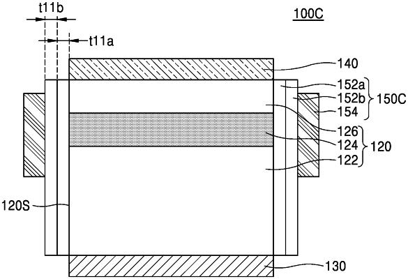
1. A semiconductor light emitting device comprising:
a light emitting structure stack comprising a first conductive semiconductor layer, a second conductive semiconductor layer, and an active layer arranged between the first conductive semiconductor layer and the second conductive semiconductor layer;
a first electrode electrically connected to the first conductive semiconductor layer;
a second electrode electrically connected to the second conductive semiconductor layer; and
a field control structure on a sidewall of the light emitting structure stack, the field control structure comprising:
a field control electrode on a sidewall of the active layer; and
a dielectric layer between the field control electrode and the active layer,
wherein the dielectric layer comprises a first dielectric layer and a second dielectric layer sequentially arranged on the sidewall of the active layer,
wherein the second dielectric layer comprises a different material than the first dielectric layer,
wherein at least one from among the first dielectric layer and the second dielectric layer is configured to act as a fixed charge layer,
wherein the first dielectric layer and the second dielectric layer have different total charge densities, and
wherein the field control electrode is configured to cause imbalance between a first carrier concentration and a second carrier concentration by bending an energy band of a portion of the active layer adjacent to an interface between the active layer and the dielectric layer.
|