| CPC H01L 31/1868 (2013.01) [H01L 31/022425 (2013.01); H01L 31/02363 (2013.01); H01L 31/1804 (2013.01); H01L 31/186 (2013.01); H01L 31/02167 (2013.01)] | 18 Claims |

|
1. A solar cell, comprising:
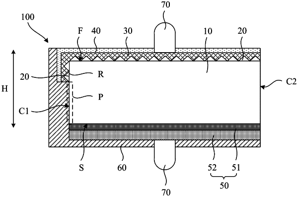
a substrate, having a first surface, a second surface, and a first side surface, the first surface and the second surface being opposite to each other, the first side surface being adjacent to and between the first surface and the second surface, and at least the first surface and a portion of the first side surface of the substrate include a textured structure;
a doped conducting layer, disposed at least on the first surface and the portion of the first side surface to cover the textured structure;
a first passivation layer, stacked on the doped conducting layer and covering the first surface and at least the portion of the first side surface, thereby covering at least the doped conducting layer;
a passivating contact layer, disposed on the second surface;
a second passivation layer, stacked on the passivating contact layer and covering the second surface, thereby covering the passivating contact layer; and
a first electrode and a second electrode, wherein the first electrode penetrates the first passivation layer and is in contact with the doped conducting layer, the second electrode penetrates the second passivation layer and is in contact with the passivating contact layer, and the first electrode and the second electrode are physically separated from the substrate, wherein the portion of the first side surface of the substrate that includes the textured structure is a textured region, and the first side surface includes a flat region adjacent to the textured region,
wherein on the first side surface, the first passivation layer completely covers the textured region and covers at least a portion of the flat region, and
wherein an edge of the first passivation layer away from the first surface is flush with a surface of the passivating contact layer away from the substrate.
|