| CPC H01L 31/022425 (2013.01) [H01L 31/0465 (2014.12); H01L 31/0352 (2013.01)] | 10 Claims |

|
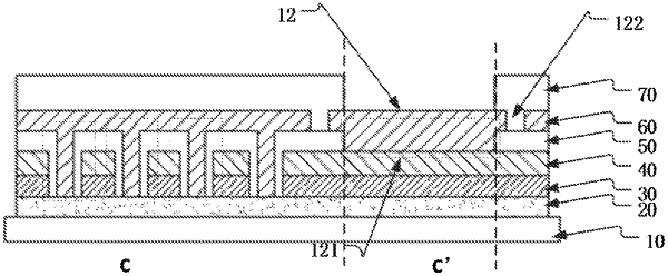
1. A thin film photovoltaic cell, wherein a film layer structure thereof is arranged in sequential attachment by:
a transparent substrate;
a transparent electrode;
a thin film photovoltaic layer;
a first metal electrode layer;
an insulating layer;
a second metal electrode layer; and
a protective layer,
the thin film photovoltaic cell comprises a power generation region, a positive electrode and a negative electrode, wherein the positive electrode and the negative electrode are respectively arranged at both ends of the power generation region, and:
the power generation region comprises first via structure patterns, and through the first via structure patterns, a transparent electrode layer and the second metal electrode layer in the power generation region are lap-jointed, and the second metal electrode layer is insulated from the thin film photovoltaic layer and the first metal electrode layer being passed;
the transparent electrode, the thin film photovoltaic layer, the first metal electrode layer, the insulating layer and the second metal electrode layer in the positive electrode are correspondingly connected with respective film layers in the power generation region, and the transparent electrode, the thin film photovoltaic layer and the first metal electrode layer in the negative electrode are correspondingly connected with the respective film layers in the power generation region; and
the negative electrode comprises a first opening structure and a second via structure pattern arranged on the insulating layer, the second metal electrode layer in the negative electrode is separated from the second metal electrode layer in the power generation region by the first opening structure, and the first metal electrode layer in the negative electrode and the second metal electrode layer are lap-jointed by the second via structure pattern,
wherein the first opening structure divides the second metal electrode layer on the insulating layer into a first part directly on and in contact with the second via structure pattern in the negative electrode and a second part separated from the first part by the first opening structure surrounding the first part and connected to the transparent electrode through the first via structure patterns in the power generation region, and
wherein the protective layer is filled in the first opening structure and comprises an opening exposing the first part.
|