| CPC H01L 29/78618 (2013.01) [H01L 21/02532 (2013.01); H01L 21/0259 (2013.01); H01L 29/0665 (2013.01); H01L 29/42392 (2013.01); H01L 29/66545 (2013.01); H01L 29/66553 (2013.01); H01L 29/66742 (2013.01); H01L 29/78696 (2013.01)] | 20 Claims |

|
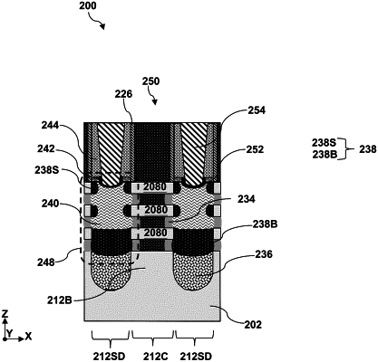
1. A method, comprising:
forming a fin-shaped structure over a substrate, the fin-shaped structure comprising a plurality of channel layers interleaved by a plurality of sacrificial layers;
recessing a source/drain region of the fin-shaped structure to form a source/drain recess that extends into the substrate and exposes a portion of the substrate;
selectively and partially recessing sidewalls of the plurality of sacrificial layers to form inner spacer recesses;
forming inner spacers in the inner spacer recesses;
selectively forming a buffer semiconductor layer on the exposed portion of the substrate;
selectively depositing a first epitaxial layer on sidewalls of the plurality of channel layer and the buffer semiconductor layer such that a top surface of the buffer semiconductor layer is completely covered by the first epitaxial layer; and
depositing a second epitaxial layer over the first epitaxial layer and the inner spacers.
|