| CPC H01L 29/7843 (2013.01) [H01L 21/0217 (2013.01); H01L 21/02208 (2013.01); H01L 21/0228 (2013.01); H01L 21/0234 (2013.01); H01L 21/3065 (2013.01); H01L 21/31155 (2013.01); H01L 21/32133 (2013.01); H01L 21/76224 (2013.01); H01L 21/823431 (2013.01); H01L 21/823437 (2013.01); H01L 21/823481 (2013.01); H01L 27/0886 (2013.01); H01L 29/66545 (2013.01); H01L 29/66795 (2013.01)] | 20 Claims |

|
1. A method comprising:
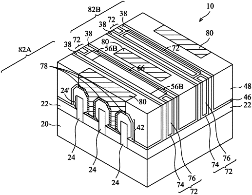
etching a dummy gate stack to reveal a protruding semiconductor fin protruding higher than isolation regions, wherein the isolation regions are over a bulk semiconductor substrate;
etching the protruding semiconductor fin;
removing portions of semiconductor materials underlying the protruding semiconductor fin to form an opening, wherein the removing is performed using the isolation regions as parts of an etching mask, and the opening extends into the bulk semiconductor substrate; and
in a process chamber, depositing a silicon nitride layer using Atomic Layer Deposition (ALD) to fill the opening, wherein the ALD comprises a plurality of ALD cycles, each comprising:
introducing a silicon-containing precursor into the process chamber;
purging the silicon-containing precursor from the process chamber;
introducing hydrogen radicals into the process chamber;
purging the hydrogen radicals from the process chamber;
introducing a nitrogen-containing precursor into the process chamber; and
purging the nitrogen-containing precursor from the process chamber.
|