| CPC H01L 29/6656 (2013.01) [H01L 21/76224 (2013.01); H01L 29/41783 (2013.01); H01L 29/511 (2013.01); H01L 29/66795 (2013.01)] | 20 Claims |

|
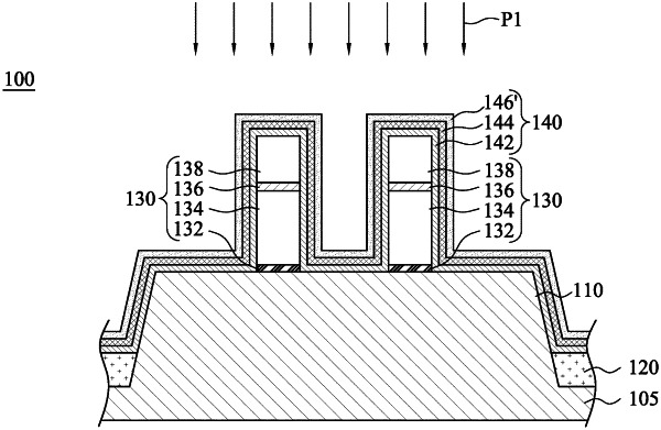
1. A method for forming a semiconductor device, comprising:
forming a gate structure on a substrate;
depositing a carbon-containing seal layer over the gate structure;
depositing a nitrogen-containing seal layer over the carbon-containing seal layer;
after depositing the nitrogen-containing seal layer over the carbon-containing seal layer, flowing an oxygen-containing precursor in a gaseous state into a process chamber, the process chamber having the substrate therein;
performing a heating treatment, by a heater, to anneal the oxygen-containing precursor to a temperature in a range from about 200 to 500° C. and under a pressure in a range from about from about 12 to 18 Torr, such that the oxygen-containing precursor is dissociated into an oxygen radical,
wherein during performing the heating treatment, the oxygen radical penetrates into the nitrogen-containing seal layer to react with the nitrogen-containing seal layer in a thickness range from an upper surface of the nitrogen-containing seal layer; and
etching the nitrogen-containing seal layer and the carbon-containing seal layer, such that a remainder of the nitrogen-containing seal layer and the carbon-containing seal layer remains on a sidewall of the gate structure as a gate spacer.
|