US 12,125,897 B2
Air spacers in transistors and methods forming same
Yi-Lun Chen, Taichung (TW); Chao-Hsien Huang, Kaohsiung (TW); Li-Te Lin, Hsinchu (TW); and Chun-Hsiung Lin, Zhubei (TW)
Assigned to TAIWAN SEMICONDUCTOR MANUFACTURING COMPANY, LTD., Hsinchu (TW)
Filed by Taiwan Semiconductor Manufacturing Co., Ltd., Hsinchu (TW)
Filed on Jun. 28, 2023, as Appl. No. 18/343,322.
Application 16/566,226 is a division of application No. 15/966,603, filed on Apr. 30, 2018, granted, now 10,861,953, issued on Dec. 8, 2020.
Application 18/343,322 is a continuation of application No. 17/201,342, filed on Mar. 15, 2021, granted, now 11,728,221.
Application 17/201,342 is a continuation of application No. 16/566,226, filed on Sep. 10, 2019, granted, now 10,964,795, issued on Mar. 30, 2021.
Prior Publication US 2023/0343649 A1, Oct. 26, 2023
Int. Cl. H01L 29/66 (2006.01); H01L 21/8234 (2006.01); H01L 21/8238 (2006.01); H01L 29/51 (2006.01); H01L 29/78 (2006.01)
CPC H01L 29/6653 (2013.01) [H01L 21/823468 (2013.01); H01L 21/823864 (2013.01); H01L 29/515 (2013.01); H01L 29/66545 (2013.01); H01L 29/66553 (2013.01); H01L 29/66795 (2013.01); H01L 29/785 (2013.01)] 20 Claims
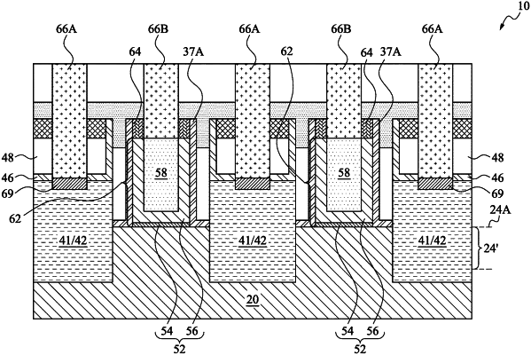
OG exemplary drawing
 
1. A device, comprising:
a gate stack;
a gate spacer on a sidewall of the gate stack, wherein the gate spacer comprises:
an inner sidewall spacer comprising a first vertical portion, wherein the first vertical portion contacts the gate stack; and
an air gap; and
a contact etch stop layer having a second vertical portion, wherein the second vertical portion of the contact etch stop layer and the first vertical portion of the inner sidewall spacer are on opposing sides of the air gap, and the air gap comprises a first portion higher than, and a second portion lower than, a bottom of the contact etch stop layer.