| CPC H01L 29/513 (2013.01) [H01L 21/28088 (2013.01); H01L 21/28185 (2013.01); H01L 29/1054 (2013.01); H01L 29/161 (2013.01); H01L 29/4966 (2013.01); H01L 29/517 (2013.01); H01L 29/66795 (2013.01); H01L 29/7851 (2013.01)] | 19 Claims |

|
1. A device comprising:
a semiconductor region;
an interfacial layer over the semiconductor region, the interfacial layer comprising a semiconductor oxide;
a high-k dielectric layer over the interfacial layer;
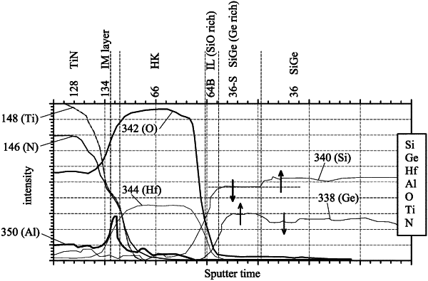
an intermixing layer over the high-k dielectric layer, wherein the intermixing layer comprises oxygen and a second metal comprising aluminum, and wherein the intermixing layer is a dielectric layer, wherein the aluminum has a peak atomic percentage in the intermixing layer and at an intermediate level between a top surface and a bottom surface of the intermixing layer, and wherein in directions pointing from the intermediate level to the top surface and pointing from the intermediate level to the bottom surface of the intermixing layer, aluminum atomic percentages reduce gradually;
a work-function layer over the intermixing layer, wherein the work-function layer is an electrically conductive layer; and
a filling-metal region over the work-function layer.
|