| CPC H01L 29/4983 (2013.01) [H01L 21/823431 (2013.01); H01L 21/823468 (2013.01); H01L 21/823821 (2013.01); H01L 21/823864 (2013.01); H01L 27/0886 (2013.01); H01L 29/0847 (2013.01); H01L 29/6653 (2013.01); H01L 29/66545 (2013.01); H01L 29/6656 (2013.01); H01L 29/66636 (2013.01); H01L 29/66795 (2013.01); H01L 29/785 (2013.01); H01L 29/7851 (2013.01)] | 20 Claims |

|
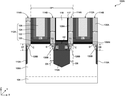
1. A semiconductor device, comprising:
a substrate;
a fin structure with a fin top surface disposed on the substrate;
a source/drain (S/D) region disposed on the fin structure;
a gate structure, disposed on the fin top surface, comprising a gate oxide layer and a high-k gate dielectric layer; and
a gate spacer with first and second spacer portions disposed between the gate structure and the S/D region,
wherein the first spacer portion extends above the fin top surface and is in contact with a sidewall of the gate oxide layer and a sidewall of the high-k gate dielectric layer,
wherein the second spacer portion extends below the fin top surface and is disposed between a sidewall of the S/D region and a sidewall of the fin structure that is facing the sidewall of the S/D region,
wherein the second spacer portion comprises a tapered structured with a first sloped sidewall adjacent to the S/D region and a second sloped sidewall adjacent to the fin structure, and
wherein an entire portion of the S/D region extending below the second spacer portion has substantially vertical sidewalls.
|
|
10. A semiconductor device, comprising:
a substrate;
a fin structure with a fin top surface disposed on the substrate;
a source/drain (S/D) region disposed within the fin structure;
a gate structure disposed on the fin top surface; and
a gate spacer with first and second spacer portions disposed between the gate structure and the S/D region,
wherein the first spacer portion is a non-tapered structure with a vertical sidewall facing the gate structure and extends above the fin top surface,
wherein the second spacer portion is a tapered structure with a first sloped sidewall facing the fin structure and a second sloped sidewall facing the S/D region and is disposed within the fin structure,
wherein an interface between the vertical sidewall and the first sloped sidewall is in contact with an interface between the gate structure and the fin structure, and
wherein an entire portion of the S/D region extending below the second spacer portion has substantially vertical sidewalls and has a bottom surface with a V-shaped cross-sectional profile.
|
|
16. A semiconductor device, comprising:
a substrate;
a source/drain (S/D) region disposed on the substrate;
a fin structure comprising a fin sidewall facing the S/D region, wherein the fin sidewall comprises a sloped sidewall portion and a vertical sidewall portion;
a gate structure disposed adjacent to the S/D region; and
a gate spacer comprising:
a first spacer portion, comprising a non-tapered cross-sectional profile, disposed along a sidewall of the gate structure, and
a second spacer portion comprising a tapered cross-sectional profile with first and second sloped spacer sidewalls,
wherein the first sloped spacer sidewall is in contact with the sloped sidewall portion of the fin sidewall and the second sloped spacer sidewall is in contact with a sidewall of the S/D region facing the fin sidewall and
wherein an entire portion of the S/D region extending below the second spacer portion has substantially vertical sidewalls.
|