| CPC H01L 29/42392 (2013.01) [H01L 21/823418 (2013.01); H01L 21/823468 (2013.01); H01L 29/0665 (2013.01); H01L 29/6656 (2013.01); H01L 29/66742 (2013.01); H01L 29/78618 (2013.01); H01L 29/78696 (2013.01)] | 20 Claims |

|
1. A method, comprising:
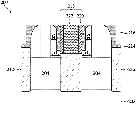
receiving a semiconductor device including a gate stack disposed over a channel region of the semiconductor device;
forming a gate spacer on a sidewall of the gate stack;
forming a source/drain feature in a source/drain region of the semiconductor device, wherein the source/drain feature is adjacent the gate spacer;
after forming the source/drain feature, performing an etch process to remove a first portion of the gate spacer, wherein a second portion of the gate spacer remains between the sidewall of the gate stack and the source/drain feature;
forming a contact etch stop layer on the gate spacer, wherein the contact etch stop layer is disposed on a top surface of the second portion of the gate spacer; and
forming a source/drain contact on the source/drain feature and adjacent the contact etch stop layer.
|