| CPC H01L 29/41725 (2013.01) [H01L 21/0254 (2013.01); H01L 29/0847 (2013.01); H01L 29/2003 (2013.01); H01L 29/205 (2013.01); H01L 29/66462 (2013.01); H01L 29/7786 (2013.01); H01L 29/7787 (2013.01)] | 20 Claims |

|
1. A device comprising:
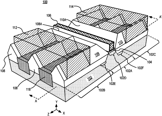
a first plurality of fins comprising a first group III-Nitride (III-N) material layer, wherein the first plurality of fins are spaced apart over a length in a first dimension;
a second plurality of fins comprising the first group III-N material layer, wherein the second plurality of fins are spaced apart along the length in the first dimension;
a central body comprising the first group III-N material layer, wherein the central body spans at least the length in the first dimension, the first plurality of fins intersect the central body on a first side, and the second plurality of fins intersect the central body on a second side, opposite the first side, and wherein the first group III-N material layer is continuous between the central body and each of the first and second pluralities of fins;
a polarization charge inducing layer above at least a portion of the central body, the polarization charge inducing layer comprising a second group III-N material of a composition that induces a 2-dimensional electron gas (2DEG) within a region of the first group III-N material layer of the central body;
a gate electrode above at least a portion of the central body;
a source structure and a drain structure comprising a third group III-N material with an impurity dopant, wherein the source structure is above, and electrically coupled to, the first plurality of fins, and wherein the drain structure is above, and electrically coupled to, the second plurality of fins;
a source contact in contact with the source structure; and
a drain contact in contact with the drain structure.
|