| CPC H01L 29/401 (2013.01) [H01L 21/28518 (2013.01); H01L 29/41791 (2013.01); H01L 29/45 (2013.01); H01L 29/66545 (2013.01); H01L 29/66795 (2013.01); H01L 29/7851 (2013.01)] | 20 Claims |

|
1. A method of forming a semiconductor device, the method comprising:
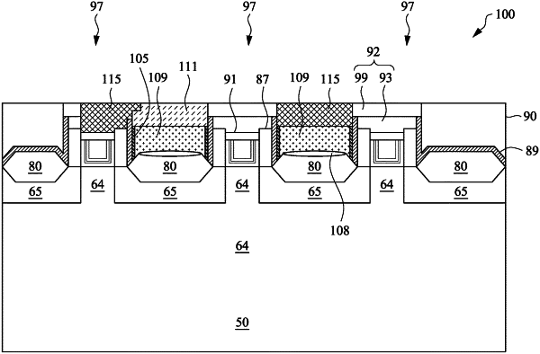
forming a metal gate structure over a fin that protrudes above a substrate, wherein the metal gate structure is surrounded by an interlayer dielectric (ILD) layer, wherein gate spacers extend along opposing sidewalls of the metal gate structure;
recessing the metal gate structure and the gate spacers below an upper surface of the ILD layer distal from the substrate, wherein recessing the metal gate structure and the gate spacers comprises:
etching back the metal gate structure using a first etching process;
after etching back the metal gate structure, recessing the gate spacers using a second etching process; and
after recessing the gate spacers, etching back the metal gate structure again using a third etching process, wherein after the third etching process, an upper surface of the metal gate structure distal from the substrate is closer to the substrate than an upper surface of the gate spacers distal from the substrate;
after the recessing, forming a first material over the metal gate structure and over the gate spacers;
after forming the first material, forming a second material over the first material, wherein an upper surface of the second material is level with the upper surface of the ILD layer;
removing a first portion of the ILD layer adjacent to the metal gate structure to form a first opening that exposes a source/drain region at a first side of the metal gate structure;
filling the first opening with a first conductive material to form a source/drain contact;
after filling the first opening, forming a gate contact over and electrically coupled to the metal gate structure, wherein the gate contact extends through the first material and the second material;
after forming the gate contact, removing the first material and the second material to form a second opening in the ILD layer; and
filling the second opening with a low-k dielectric material.
|