| CPC H01L 27/1464 (2013.01) [H01L 27/14603 (2013.01); H01L 27/14605 (2013.01); H01L 27/14683 (2013.01); H01L 27/14627 (2013.01); H01L 27/1463 (2013.01); H01L 27/14636 (2013.01); H01L 27/14806 (2013.01); H01L 27/14812 (2013.01)] | 20 Claims |

|
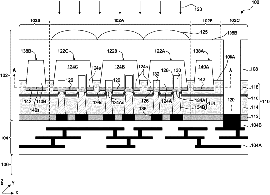
1. A method, comprising:
depositing a dielectric layer on a substrate;
forming a dummy epitaxial structure and an active epitaxial structure in the dielectric layer and the substrate;
forming first and second capping layers on the dummy and active epitaxial structures, respectively;
doping the active epitaxial structure and the second capping layer;
forming a silicide layer on the doped regions;
depositing an etch stop layer on the silicide layer; and
forming conductive plugs on the silicide layer through the etch stop layer.
|