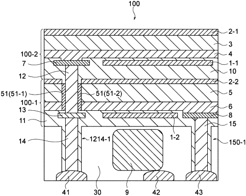
| CPC H01L 27/14603 (2013.01) [H01L 27/14609 (2013.01); H01L 27/14623 (2013.01); H01L 27/14636 (2013.01); H04N 25/77 (2023.01)] | 20 Claims |

|
1. A solid-state imaging device, comprising:
a semiconductor substrate including a charge accumulation unit;
a first photoelectric conversion unit, on the semiconductor substrate, configured to convert first light into a first charge;
a second photoelectric conversion unit, on the first photoelectric conversion unit, configured to convert second light into a second charge, wherein
each of the first photoelectric conversion unit and the second photoelectric conversion unit includes at least:
a first electrode,
a second electrode, and
a photoelectric conversion film between the first electrode and the second electrode;
a conductive portion configured to penetrate the first photoelectric conversion unit, wherein
the first electrode of the second photoelectric conversion unit and the charge accumulation unit in the semiconductor substrate are electrically connected to each other via the conductive portion; and
an insulation film portion at least on a part of an outer circumference of the conductive portion, wherein
the insulation film portion is configured to cover the outer circumference of the conductive portion,
the insulation film portion includes a first insulation film,
the first insulation film has fixed charge of a type identical to a type of charge accumulated in the charge accumulation unit,
the first insulation film is between the conductive portion and the first photoelectric conversion unit, and
the first insulation film is in direct contact with the first photoelectric conversion unit.
|