| CPC H01L 27/1248 (2013.01) [G02F 1/13338 (2013.01); G02F 1/133512 (2013.01); G02F 1/1337 (2013.01); G02F 1/134372 (2021.01); G02F 1/136204 (2013.01); G02F 1/136227 (2013.01); G02F 1/136286 (2013.01); G02F 1/1368 (2013.01); G06F 3/0412 (2013.01); G06F 3/04164 (2019.05); G06F 3/0446 (2019.05)] | 8 Claims |

|
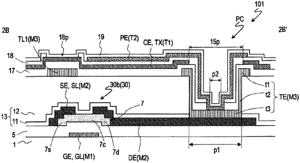
1. An active matrix substrate comprising;
a substrate;
a plurality of thin film transistors supported by the substrate, each of the plurality of thin film transistors including an oxide semiconductor layer;
an interlayer insulating layer covering the plurality of thin film transistors;
a plurality of pixel electrodes provided above the interlayer insulating layer, each of the plurality of pixel electrodes being electrically connected to a corresponding one of the plurality of thin film transistors;
a common electrode provided between the plurality of pixel electrodes and the interlayer insulating layer;
a first dielectric layer provided between the common electrode and the plurality of pixel electrodes; and
an alignment film covering the plurality of pixel electrodes, wherein:
the first dielectric layer includes a plurality of openings,
each of the plurality of openings exposes a part of the common electrode,
each of the plurality of openings includes the alignment film positioned in each opening, and
each of the plurality of openings further includes a portion overlapping the common electrode and a portion not overlapping the common electrode when viewed from a direction normal to the substrate.
|