US 12,125,852 B2
Multi-gate transistors with backside power rail and reduced gate-drain capacitance
Huan-Chieh Su, Changhua County (TW); Li-Zhen Yu, Hsinchu (TW); Chun-Yuan Chen, Hsinchu (TW); Shih-Chuan Chiu, Hsinchu (TW); Cheng-Chi Chuang, New Taipei (TW); Yu-Ming Lin, Hsinchu (TW); and Chih-Hao Wang, Hsinchu County (TW)
Assigned to TAIWAN SEMICONDUCTOR MANUFACTURING CO., LTD., Hsinchu (TW)
Filed by Taiwan Semiconductor Manufacturing Co., Ltd., Hsinchu (TW)
Filed on Jul. 28, 2023, as Appl. No. 18/360,895.
Application 18/360,895 is a continuation of application No. 17/572,212, filed on Jan. 10, 2022, granted, now 11,804,486.
Application 17/572,212 is a continuation of application No. 16/901,963, filed on Jun. 15, 2020, granted, now 11,222,892, issued on Jan. 11, 2022.
Prior Publication US 2023/0387115 A1, Nov. 30, 2023
Int. Cl. H01L 27/088 (2006.01); H01L 21/027 (2006.01); H01L 21/306 (2006.01); H01L 21/308 (2006.01)
CPC H01L 27/0886 (2013.01) [H01L 21/0274 (2013.01); H01L 21/30604 (2013.01); H01L 21/3086 (2013.01)] 20 Claims
OG exemplary drawing
 
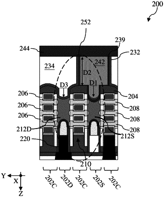
1. A structure, comprising:
an isolation feature;
a first dielectric fin, a second dielectric fin and a third dielectric fin disposed over the isolation feature;
a first epitaxial feature sandwiched between the first dielectric fin and the second dielectric fin;
a second epitaxial feature sandwiched between the second dielectric fin and the third dielectric fin;
a backside dielectric plug extending through the isolation feature to contact the first epitaxial feature; and
a backside contact extending through the isolation feature to contact the second epitaxial feature by way of a silicide layer.