| CPC H01L 27/0886 (2013.01) [H01L 21/76897 (2013.01); H01L 21/823814 (2013.01); H01L 21/823821 (2013.01); H01L 21/823842 (2013.01); H01L 23/522 (2013.01); H01L 23/528 (2013.01); H01L 27/0207 (2013.01); H01L 29/785 (2013.01); H10B 12/31 (2023.02); H10B 12/36 (2023.02); H01L 27/0924 (2013.01); H10B 12/34 (2023.02); H10B 12/37 (2023.02)] | 20 Claims |

|
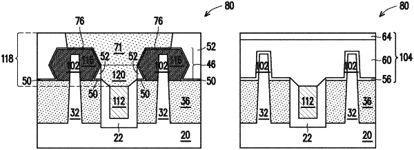
1. An integrated circuit comprising:
a bulk semiconductor substrate;
an isolation region over the bulk semiconductor substrate;
a first semiconductor fin over the isolation region;
a buried conductive track comprising at least a portion in the isolation region;
a transistor comprising:
a gate electrode over the first semiconductor fin;
a source/drain region on a side of the gate electrode, wherein the buried conductive track extends underlying the gate electrode, and at least a portion of the buried conductive track is lower than the source/drain region, and wherein the buried conductive track is connected to at least one of the gate electrode and the source/drain region;
a source/drain contact plug extending down to physically contact the buried conductive track; and
a source/drain silicide region between and contacting the source/drain contact plug and the source/drain region; and
a dielectric layer comprising:
a bottom portion directly underlying the buried conductive track; and
sidewall portions on opposing sides of, and contacting sidewalls of, the buried conductive track.
|