| CPC H01L 27/0716 (2013.01) [H01L 29/41708 (2013.01); H01L 29/7395 (2013.01); H01L 29/868 (2013.01); H01L 29/0692 (2013.01)] | 20 Claims |

|
1. A semiconductor device, comprising:
a first electrode;
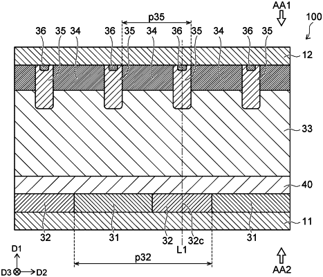
a plurality of first semiconductor regions of a first conductivity type on the first electrode, the first semiconductor regions being spaced from each other in a first direction and extending in a second direction perpendicular to the first direction;
a plurality of second semiconductor regions of a second conductivity type on the first electrode, each second semiconductor region being adjacent to at least one of the first semiconductor regions in the first direction and extending in the second direction;
a third semiconductor region of the first conductivity type on the plurality of first semiconductor regions and the plurality of second semiconductor regions and having a dopant concentration of the first conductivity type that is less than that of the plurality of first semiconductor regions, the plurality of first semiconductor regions and the plurality of second semiconductor regions being between the third semiconductor region and the first electrode in a third direction orthogonal to the first and second directions;
a plurality of fourth semiconductor regions of the second conductivity type on the third semiconductor region, spaced from each other in the first direction, and extending in the second direction;
a plurality of fifth semiconductor regions of the second conductivity type on the third semiconductor region, the fifth semiconductor regions being adjacent to at least one fourth semiconductor region in the first direction, extending in the second direction, and having a dopant concentration of the second conductivity type that is greater than that of the plurality of fourth semiconductor regions; and
a second electrode on the plurality of fourth semiconductor regions and the plurality of fifth semiconductor regions, wherein
each second semiconductor region is directly below one of the plurality of fifth semiconductor regions in the third direction, and
each fifth semiconductor region has a maximum width in the first direction that is less than a maximum width of each second semiconductor region in the first direction.
|