| CPC H01L 25/167 (2013.01) [G01J 1/0214 (2013.01); G01J 3/0227 (2013.01); G01J 3/0256 (2013.01); G01J 3/0262 (2013.01); G01J 3/108 (2013.01); G01S 7/4813 (2013.01); G01S 17/04 (2020.01); H01L 25/50 (2013.01); H01L 2924/0002 (2013.01)] | 18 Claims |

|
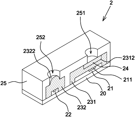
1. A module package, comprising:
a circuit board having an upper surface;
a photo sensor chip attached to the upper surface of the circuit board;
a light emitting die attached to the upper surface of the circuit board;
a first transparent layer covering the photo sensor chip and a part of the upper surface of the circuit board, wherein the first transparent layer has a receptacle opposite to the photo sensor chip;
a second transparent layer covering the light emitting die and another part of the upper surface of the circuit board;
an opaque layer covering the first transparent layer and having a through hole opposite to the receptacle; and
a filter accommodated in the receptacle, and secured by transparent adhesive in the receptacle of the first transparent layer.
|