US 12,125,828 B2
Carrying substrate, electronic package having the carrying substrate, and methods for manufacturing the same
Chi-Ching Ho, Taichung (TW); Bo-Hao Ma, Taichung (TW); Yu-Ting Xue, Taichung (TW); Ching-Hung Tseng, Taichung (TW); Guan-Hua Lu, Taichung (TW); and Hong-Da Chang, Taichung (TW)
Assigned to SILICONWARE PRECISION INDUSTRIES CO., LTD., Taichung (TW)
Filed by SILICONWARE PRECISION INDUSTRIES CO., LTD., Taichung (TW)
Filed on Sep. 11, 2023, as Appl. No. 18/464,855.
Application 18/464,855 is a continuation of application No. 16/554,779, filed on Aug. 29, 2019, granted, now 11,923,337.
Claims priority of application No. 108115386 (TW), filed on May 3, 2019; and application No. 108126794 (TW), filed on Jul. 29, 2019.
Prior Publication US 2023/0420420 A1, Dec. 28, 2023
Int. Cl. H01L 25/065 (2023.01); H01L 21/48 (2006.01); H01L 21/56 (2006.01); H01L 23/00 (2006.01); H01L 23/31 (2006.01); H01L 23/522 (2006.01)
CPC H01L 25/0657 (2013.01) [H01L 21/486 (2013.01); H01L 21/4882 (2013.01); H01L 21/563 (2013.01); H01L 23/3114 (2013.01); H01L 23/5226 (2013.01); H01L 24/13 (2013.01); H01L 2225/06541 (2013.01)] 12 Claims
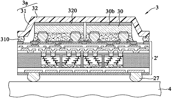
OG exemplary drawing
 
1. A carrying substrate, comprising:
a first circuit structure having a first side and a second side opposing the first side;
at least four circuit components disposed on the first side of the first circuit structure;
an encapsulation layer formed on the first side of the first circuit structure and encapsulating the at least four circuit components;
a second circuit structure formed on the encapsulation layer and electrically connected to the at least four circuit components; and
a plurality of conductive pillars disposed in the encapsulation layer and electrically connecting the first circuit structure and the second circuit structure.