| CPC H01L 25/0655 (2013.01) [H01L 23/3675 (2013.01); H01L 23/49822 (2013.01); H01L 23/49833 (2013.01); H01L 23/49838 (2013.01); H01L 24/32 (2013.01); H01L 27/0727 (2013.01); H01L 2224/32225 (2013.01); H01L 2924/1811 (2013.01); H01L 2924/1815 (2013.01); H01L 2924/182 (2013.01)] | 15 Claims |

|
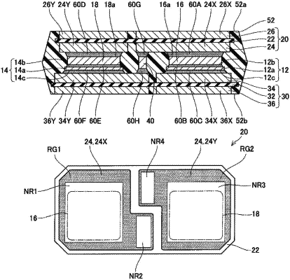
1. A semiconductor device comprising:
a first insulating substrate; and
a first semiconductor element configured to be joined to the first insulating substrate through a first conductive spacer;
wherein the first insulating substrate includes a first insulating layer and a first inner conductive layer disposed at a side of the first insulating layer,
wherein the first inner conductive layer includes a surface having a first region and a second region, and the second region surrounds the first region and has larger surface roughness than the first region,
wherein the first conductive spacer is joined to the first region of the first inner conductive layer through a first junction layer,
wherein a margin of the first region with respect to the first conductive spacer is partially enlarged in a plan view of the first inner conductive layer, and
wherein a distance between the first conductive spacer and a peripheral edge of the first inner conductive layer is larger in a portion where the margin is larger as compared with another portion where the margin is smaller.
|