| CPC H01L 24/94 (2013.01) [H01L 23/481 (2013.01); H01L 24/03 (2013.01); H01L 24/05 (2013.01); H01L 24/08 (2013.01); H01L 24/27 (2013.01); H01L 24/29 (2013.01); H01L 24/32 (2013.01); H01L 24/83 (2013.01); H01L 24/92 (2013.01); H01L 24/96 (2013.01); H01L 25/0657 (2013.01); H01L 25/18 (2013.01); H01L 25/50 (2013.01); H01L 21/304 (2013.01); H01L 21/30625 (2013.01); H01L 21/76898 (2013.01); H01L 24/06 (2013.01); H01L 24/33 (2013.01); H01L 2224/03845 (2013.01); H01L 2224/0557 (2013.01); H01L 2224/06181 (2013.01); H01L 2224/08146 (2013.01); H01L 2224/27831 (2013.01); H01L 2224/2784 (2013.01); H01L 2224/27845 (2013.01); H01L 2224/29005 (2013.01); H01L 2224/29011 (2013.01); H01L 2224/29016 (2013.01); H01L 2224/32145 (2013.01); H01L 2224/33181 (2013.01); H01L 2224/80203 (2013.01); H01L 2224/80895 (2013.01); H01L 2224/83203 (2013.01); H01L 2224/83896 (2013.01); H01L 2224/9211 (2013.01); H01L 2225/06544 (2013.01)] | 20 Claims |

|
1. A package component comprising:
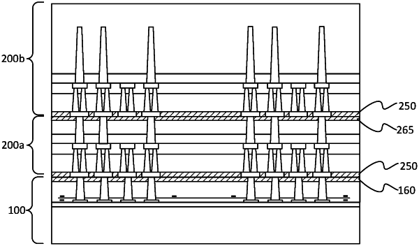
a first device bonded to a second device, wherein the first device comprises a semiconductor substrate, a first insulating bonding layer on a first surface of the semiconductor substrate, a first interconnect on a second surface of the semiconductor substrate, and metal vias extending through the semiconductor substrate, the first insulating bonding layer, and the first interconnect, wherein the second device comprises a second insulating bonding layer and bond pads in the second insulating bonding layer, wherein at a bonding interface between the first device and the second device the metal vias of the first device are directly bonded to the bond pads of the second device and the first insulating bonding layer of the first device is fused to the second insulating bonding layer of the second device, the first insulating bonding layer disposed at a back side of the first device.
|