| CPC H01L 24/08 (2013.01) [H01L 23/36 (2013.01); H01L 23/5226 (2013.01); H01L 24/80 (2013.01); H01L 2224/08145 (2013.01); H01L 2224/80895 (2013.01); H01L 2224/80896 (2013.01)] | 20 Claims |

|
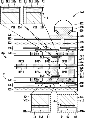
1. An integrated circuit package, comprising:
a first semiconductor die, comprising:
a plurality of first die pads over a first device;
a plurality of first bonding pads over the first die pads;
a first conductive via disposed between and electrically connected to a first one of the first die pads and a first one of the first bonding pads; and
a first thermal via disposed between a second one of the first die pads and a second one of the first bonding pads and electrically insulated from the second one of the first die pads or the second one of the first bonding pads; and
a second semiconductor die bonded to the first semiconductor die and comprising:
a plurality of second bonding pads, wherein the first one of the first bonding pads is connected to a first one of the second bonding pads, and the second one of the first bonding pads is connected to a second one of the second bonding pads.
|