| CPC H01L 24/04 (2013.01) [H01L 24/03 (2013.01); H01L 24/13 (2013.01); H01L 2224/02206 (2013.01); H01L 2224/02311 (2013.01); H01L 2224/02331 (2013.01); H01L 2224/0235 (2013.01); H01L 2224/02373 (2013.01); H01L 2224/02375 (2013.01); H01L 2224/0239 (2013.01); H01L 2224/024 (2013.01); H01L 2224/03013 (2013.01); H01L 2224/0312 (2013.01); H01L 2224/0401 (2013.01); H01L 2224/05147 (2013.01); H01L 2224/05666 (2013.01); H01L 2224/13014 (2013.01); H01L 2224/13024 (2013.01); H01L 2924/014 (2013.01)] | 16 Claims |

|
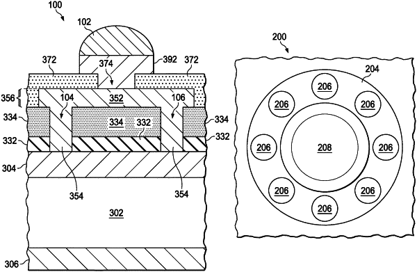
1. A semiconductor structure comprising:
a metal layer;
a passivation layer disposed on the metal layer;
a first polyimide layer disposed on the passivation layer;
a redistribution layer (RDL) structure comprising:
an RDL platform disposed on the first polyimide layer; and
a plurality of RDL pillars extending between the RDL platform and the metal layer wherein:
the plurality of RDL pillars extend through the passivation layer and the first polyimide layer; and
the plurality of RDL pillars are separated from each other by the passivation layer and the first polyimide layer;
a second polyimide layer disposed on the RDL platform, the second polyimide layer having a cavity defined therein;
an under-bump metal (UBM) disposed on the RDL platform that includes a substantially planar topmost surface that extends across the cavity such that the UBM completely fills the cavity and extends across a topmost surface of the second polyimide layer beyond the cavity; and
a solder bump disposed on the UBM, wherein the UBM, the RDL platform, and the RDL pillars form an electrical connection between the solder bump and the metal layer, and wherein:
the plurality of RDL pillars are disposed in a ring around the solder bump; and
the plurality of RDL pillars includes a first pillar and a second pillar disposed away from and on opposite sides of a region of the first polyimide layer directly underneath the UBM such that none of the plurality of RDL pillars is directly underneath the UBM.
|