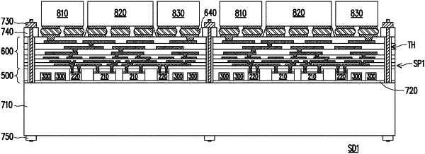
| CPC H01L 23/562 (2013.01) [H01L 21/4853 (2013.01); H01L 21/4857 (2013.01); H01L 21/561 (2013.01); H01L 21/565 (2013.01); H01L 21/568 (2013.01); H01L 21/6835 (2013.01); H01L 23/3128 (2013.01); H01L 23/4006 (2013.01); H01L 23/5383 (2013.01); H01L 23/5386 (2013.01); H01L 24/96 (2013.01); H01L 25/0655 (2013.01); H01L 25/50 (2013.01); H01L 2023/4031 (2013.01); H01L 2023/405 (2013.01); H01L 2023/4087 (2013.01); H01L 2221/68372 (2013.01); H01L 2224/95001 (2013.01); H01L 2924/3511 (2013.01)] | 20 Claims |

|
1. A semiconductor package, having a central region and a peripheral region surrounding the central region, the semiconductor package comprising:
a plurality of pairs of first functional dies disposed in the center region; and
a plurality of first dummy dies disposed in the peripheral region,
wherein a size of the first functional dies is different from a size of the first dummy dies,
wherein an outmost pair of first functional dies is spaced from an edge of the semiconductor package by a non-zero distance, and
wherein each pair of first functional dies is encapsulated by a first encapsulant, the first encapsulant is encapsulated by a second encapsulant, and the second encapsulant is different from the first encapsulant.
|