| CPC H01L 23/5386 (2013.01) [H01L 21/4857 (2013.01); H01L 21/486 (2013.01); H01L 21/561 (2013.01); H01L 21/566 (2013.01); H01L 21/6835 (2013.01); H01L 23/5383 (2013.01); H01L 23/5384 (2013.01); H01L 23/5389 (2013.01); H01L 24/18 (2013.01); H01L 24/19 (2013.01); H01L 24/20 (2013.01); H01L 25/0657 (2013.01); H01L 21/568 (2013.01); H01L 23/3128 (2013.01); H01L 23/49816 (2013.01); H01L 23/49827 (2013.01); H01L 25/105 (2013.01); H01L 25/50 (2013.01); H01L 2221/68345 (2013.01); H01L 2221/68359 (2013.01); H01L 2221/68372 (2013.01); H01L 2221/68381 (2013.01); H01L 2224/04105 (2013.01); H01L 2224/12105 (2013.01); H01L 2224/16227 (2013.01); H01L 2224/18 (2013.01); H01L 2224/24227 (2013.01); H01L 2224/32225 (2013.01); H01L 2224/73267 (2013.01); H01L 2224/92244 (2013.01); H01L 2224/97 (2013.01); H01L 2225/1035 (2013.01); H01L 2225/1041 (2013.01); H01L 2225/1058 (2013.01); H01L 2924/1203 (2013.01); H01L 2924/1304 (2013.01); H01L 2924/13091 (2013.01); H01L 2924/1431 (2013.01)] | 20 Claims |

|
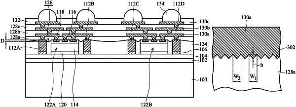
1. A package structure, comprising:
a semiconductor chip;
a first dielectric layer over the semiconductor chip and extending across opposite sidewalls of the semiconductor chip, wherein the first dielectric layer has scratches;
a conductive layer over the first dielectric layer, wherein the conductive layer extends across a first plurality of the scratches; and
a second dielectric layer over the conductive layer and extending across a second plurality of the scratches, wherein the second dielectric layer extends into the second plurality of the scratches, and bottoms of the second plurality of the scratches are positioned at height levels that are lower than an upper surface of the first dielectric layer.
|