| CPC H01L 23/535 (2013.01) [H01L 21/76895 (2013.01); H01L 21/823475 (2013.01); H01L 23/5221 (2013.01); H01L 23/528 (2013.01); H01L 23/5286 (2013.01); H01L 23/5386 (2013.01); H01L 27/0207 (2013.01); H01L 29/401 (2013.01); H01L 29/41725 (2013.01)] | 20 Claims |

|
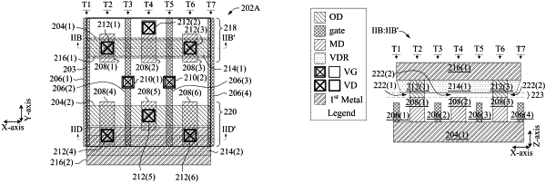
1. A method of forming a semiconductor device, the method comprising:
forming an active region;
forming first, second and third metal-to-drain/source (MD) contact structures which extend in a first direction, and correspondingly overlap and electrically couple to the active region;
forming a first via-to-MD (VD) structure over, and electrically coupled to, the first MD contact structure;
forming a via-to-via (V2V) rail which extends in a second direction perpendicular to the first direction, overlaps the first MD contact structure and at least one of the second or third MD contact structures, and is electrically coupled to the first VD structure;
relative to a third direction which is perpendicular to each of the first and second directions:
setting an upper surface of the V2V rail so as to not project beyond an upper surface of the first VD structure; and
setting a lower surface of the V2V rail so that first, second and third gaps remain correspondingly between the lower surface of the V2V rail and upper surfaces correspondingly of first, second and third MD contact structures; and
forming a first conductive segment which overlaps the V2V rail, is in a first metallization layer, and is electrically coupled to the first VD structure, and
wherein at least one of the second and third MD contact structures is electrically decoupled from the V2V rail correspondingly by the second or third gaps.
|