| CPC H01L 23/5283 (2013.01) [H01L 21/76816 (2013.01); H01L 21/76877 (2013.01); H01L 23/5226 (2013.01); H10B 43/50 (2023.02); H10B 41/00 (2023.02); H10B 41/35 (2023.02); H10B 41/50 (2023.02); H10B 43/35 (2023.02)] | 20 Claims |

|
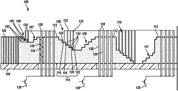
1. A device, comprising:
a stack comprising tiers each comprising conductive material and SiO2 vertically neighboring the conductive material;
stair step structures comprising steps defined by ends of at least some of the tiers;
a landing interposed between two of the stair step structures, the landing comprising:
an outer region comprising a portion of the stack comprising the tiers each comprising the conductive material and the SiO2 vertically adjacent the conductive material; and
an inner region horizontally surrounded by the outer region and comprising:
additional tiers each comprising Si3N4 and additional SiO2 vertically alternating with the Si3N4; and
vias vertically extending through the Si3N4 and the additional SiO2;
conductive contacts extending through the vias of the inner region of the landing, the conductive contacts electrically coupled to access lines electrically coupled to memory cells; and
a control unit for controlling the memory cells, the control unit positioned proximate the landing and electrically coupled to one or more of the conductive contacts within one or more of the vias within the landing.
|