| CPC H01L 23/4006 (2013.01) [H01L 21/4871 (2013.01); H01L 2023/4087 (2013.01)] | 14 Claims |

|
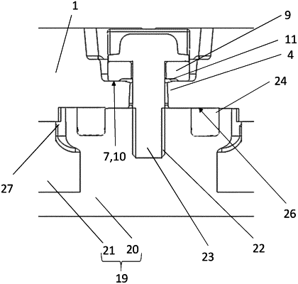
1. A clamping element configured to be pressed to a baseplate of at least one power semiconductor module comprising a mold, comprising
at least two contact areas being configured to be in direct contact to at least one clamping area of the baseplate being free of the mold, and
at least two recesses provided in the clamping element,
at least two holes, wherein
at least one recess and at least one contact area are configured to face the baseplate,
the clamping element is configured to connect the at least one power semiconductor module with a cooler.
|