| CPC H01L 21/7682 (2013.01) [H01L 21/76828 (2013.01); H01L 21/76829 (2013.01); H01L 21/76841 (2013.01); H01L 21/76895 (2013.01); H01L 23/5329 (2013.01); H01L 23/535 (2013.01); H10B 12/00 (2023.02)] | 13 Claims |

|
1. A semiconductor device, comprising:
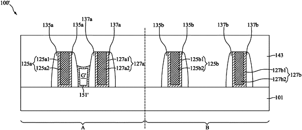
a first conductive feature and a second conductive feature disposed over a pattern-dense region of a semiconductor substrate;
a third conductive feature and a fourth conductive feature disposed over a pattern-loose region of the semiconductor substrate; and
a dielectric layer disposed over the pattern-dense region and the pattern-loose region of the semiconductor substrate, wherein a first portion of the dielectric layer between the first conductive feature and the second conductive feature is separated from the semiconductor substrate by an air gap, and a second portion of the dielectric layer between the third conductive feature and the fourth conductive feature is in direct contact with the semiconductor substrate;
wherein at least one of the first conductive feature, the second conductive feature, the third conductive feature and the fourth conductive feature is a composite feature including a protection liner and a plug in the protection liner, wherein a top surface of the plug is exposed from the protection liner and a top surface of the protection liner is in contact with the dielectric layer;
wherein the top surface of the protection liner is higher than a bottom surface of the first portion of the dielectric layer.
|