| CPC H01L 21/76816 (2013.01) [H01L 21/02063 (2013.01); H01L 21/31116 (2013.01); H01L 21/76834 (2013.01); H01L 23/5226 (2013.01); H01L 23/5283 (2013.01); H01L 23/53266 (2013.01); H10B 10/12 (2023.02)] | 20 Claims |

|
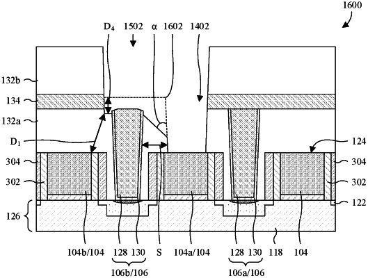
1. An integrated circuit (IC) comprising:
a substrate;
a source/drain region overlying and inset into a top of the substrate;
a gate electrode bordering the source/drain region and located over the substrate;
a first level contact overlying and electrically coupled to the source/drain region;
a second level contact overlying the first level contact and the gate electrode; and
a gate via extending from the second level contact to the gate electrode, wherein a height of the second level contact increases from the first level contact to the gate via.
|
|
8. An integrated circuit (IC) comprising:
a substrate;
a device overlying the substrate and comprising a gate electrode;
an active region (AR) contact extending along a sidewall of the gate electrode, from the substrate to an elevation above a top surface of the gate electrode; and
a gate-to-contact (GC) structure overlying the AR contact and the gate electrode, wherein the GC structure extends from the top surface of the gate electrode to a top surface of the AR contact, and comprises a gate via extending to the top surface of the gate electrode and spaced from the AR contact, and wherein the GC structure has a sidewall facing the AR contact at the gate via and with a top edge recessed relative to the top surface of the AR contact.
|
|
15. An integrated circuit (IC) comprising:
a substrate;
a gate electrode overlying the substrate;
a first active region (AR) contact extending from the substrate;
a gate contact overlying the gate electrode and the first AR contact; and
a gate via extending from the gate contact to the gate electrode; and
an etch stop layer overlying the gate electrode and having a bottom surface elevated relative to a top surface of the first AR contact;
wherein the gate contact extends through the etch stop layer and has a top surface elevated relative to a top surface of the etch stop layer.
|