| CPC H01L 21/76807 (2013.01) [H01L 21/02645 (2013.01); H01L 21/56 (2013.01); H01L 21/78 (2013.01); H01L 23/3114 (2013.01); H01L 23/5329 (2013.01); H01L 23/5384 (2013.01); H01L 24/32 (2013.01); H01L 2221/1015 (2013.01); H01L 2224/0231 (2013.01); H01L 2224/32225 (2013.01); H01L 2924/14 (2013.01)] | 20 Claims |

|
1. A method of forming a semiconductor structure, comprising:
providing a substrate having at least one contact therein and a dielectric material layer thereon;
performing a double exposure process to the dielectric material layer including sequentially performing a first exposure process to form first exposure portions in the dielectric material layer and performing a second exposure process to form second exposure portions in the dielectric material layer;
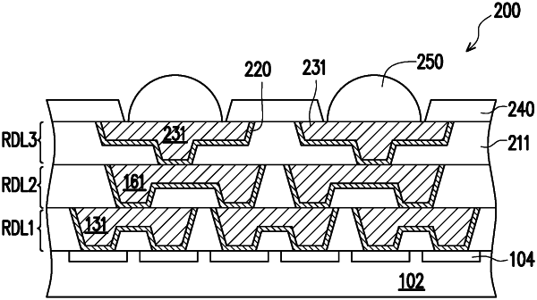
performing a development process to dissolve the first and second exposure portions and over-develop the dielectric material layer to form a dual damascene opening with a via opening and a trench opening communicated with the via opening, wherein a slant sidewall of the via opening is connected with a slant sidewall of the trench opening, and the slant sidewall of the via opening has the same slope as the slant sidewall of the trench opening;
forming a seed metallic layer into the dual damascene opening and over the dielectric material layer; and
forming a metallic pattern filled in the dual damascene opening.
|