| CPC H01L 21/4853 (2013.01) [H01L 23/49827 (2013.01); H01L 23/49838 (2013.01); H01L 23/49866 (2013.01); H01L 24/16 (2013.01); H01L 24/81 (2013.01); H01L 2224/16227 (2013.01); H01L 2224/81035 (2013.01); H01L 2224/81047 (2013.01); H01L 2224/81192 (2013.01); H01L 2224/81395 (2013.01); H01L 2224/81411 (2013.01); H01L 2224/81444 (2013.01); H01L 2224/81447 (2013.01); H01L 2224/81455 (2013.01); H01L 2224/81493 (2013.01)] | 20 Claims |

|
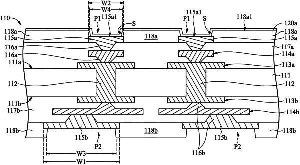
1. A chip package structure, comprising:
a wiring substrate comprising a substrate, a first pad, and a second pad, wherein the first pad and the second pad are respectively over a first surface and a second surface of the substrate, and the first pad is narrower than the second pad;
a nickel layer over the first pad, wherein the nickel layer has a T-shape in a cross-sectional view of the nickel layer;
a chip over the wiring substrate;
a conductive bump between the nickel layer and the chip; and
a conductive adhesive layer over the first pad, wherein the nickel layer is over the conductive adhesive layer, the nickel layer has a first lower surface and a bottom surface, the first lower surface is higher than the bottom surface, the conductive adhesive layer has a second lower surface, and the first lower surface is substantially level with the second lower surface.
|