| CPC H01L 21/31144 (2013.01) [H01L 21/76808 (2013.01); H01L 21/76877 (2013.01); H01L 23/5226 (2013.01); H01L 23/528 (2013.01)] | 20 Claims |

|
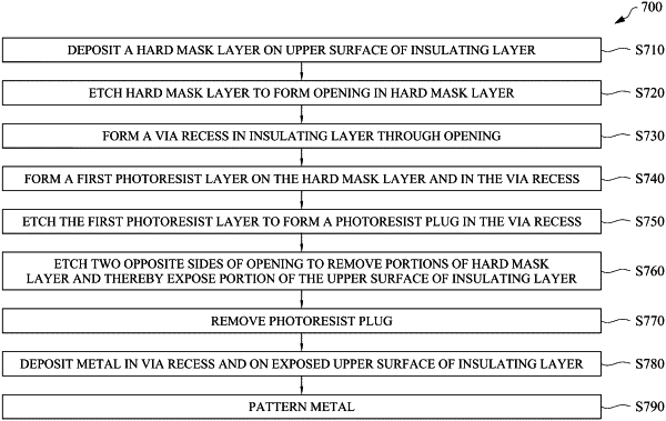
1. A method, comprising:
depositing a hard mask layer on an upper surface of an insulating layer;
etching the hard mask layer to form an opening in the hard mask layer;
forming a via recess in the hard mask layer through the opening;
forming a first photoresist layer on the hard mask layer and in the via recess;
etching the first photoresist layer to form a photoresist plug in the via recess;
etching two opposite sides of the opening to remove portions of the hard mask layer and thereby expose a portion of the upper surface of the insulating layer;
removing the photoresist plug;
depositing metal in the via recess, in the opening, and on the exposed upper surface of the insulating layer; and
patterning the metal over the via recess to form a metal line that is in contact with at least the metal in the opening, wherein an axis of the metal line is offset from the center of the via recess.
|