| CPC H01L 21/28185 (2013.01) [H01L 21/02356 (2013.01); H01L 21/28158 (2013.01); H01L 21/3115 (2013.01); H01L 21/823431 (2013.01); H01L 21/823462 (2013.01); H01L 29/517 (2013.01); H01L 29/66795 (2013.01); H01L 29/785 (2013.01)] | 20 Claims |

|
1. A method comprising:
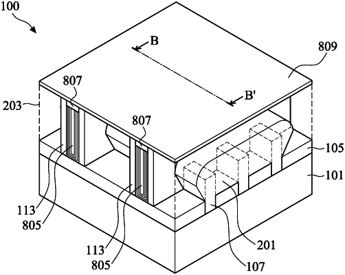
forming a gate dielectric layer over a top surface and sidewalls of a semiconductor fin, wherein the gate dielectric layer comprises a plurality of nano-crystallite regions suspended within an amorphous matrix material, wherein the amorphous matrix material separates grain boundaries of the plurality of nano-crystallite regions, and wherein the plurality of nano-crystallite regions have a first crystalline phase;
performing a first anneal process to modify the first crystalline phase of the plurality of nano-crystallite regions to a second crystalline phase that is different from the first crystalline phase;
forming a capping layer over the gate dielectric layer after the first anneal process; and
performing a second anneal process to further crystallize the plurality of nano-crystallite regions.
|