| CPC H01L 21/0272 (2013.01) [H01L 21/02126 (2013.01); H01L 21/31051 (2013.01); H01L 21/7624 (2013.01)] | 8 Claims |

|
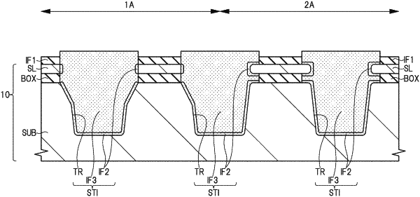
1. A method of manufacturing a semiconductor device having a first region in which a first MISFET is to be formed and a second region in which a second MISFET is to be formed, comprising:
(a) preparing an SOI substrate having a semiconductor substrate, an insulating layer formed on the semiconductor substrate, and a semiconductor layer formed on the insulating layer;
(b) after the step (a), in each of the first region and the second region, forming a first insulting film on the semiconductor layer, the first insulating film being made of a material different from a material of the insulating layer;
(c) after the (b), in each of the first region and the second region, forming a mask pattern by pattering the first insulating film;
(d) after the (c), in each of the first region and the second region, forming a plurality of trenches each reaching an inside of the semiconductor substrate by performing an etching process with the mask pattern as a mask, and exposing each of a side surface of the semiconductor layer, a side surface of insulating layer and a side surface of the semiconductor substrate in an inside of each of the plurality of trenches;
(e) after the (d), in each of the first region and the second region, retreating the side surface of the insulating layer from the side surface of the semiconductor layer and the side surface of the semiconductor substrate by cleaning the inside of each of the plurality of trenches;
(f) after the (e), in each of the first region and the second region, embedding an organic film into the inside of each of the plurality of trenches;
(g) after the (f), covering the side surface of the insulating layer in the first region with the organic film and also exposing the side surface of the semiconductor layer in the first region from the organic film by performing an anisotropic etching process to the organic film in the first region;
(h) after the (g), in each of the first region and the second region, approaching each of the side surface of the semiconductor layer in the first region and the side surface of the semiconductor substrate in the first region to the side surface of the insulating layer in the first region by performing an anisotropic etching process, the isotropic etching process having a condition in which the organic film, the semiconductor layer and the semiconductor substrate are more easily etched than the insulating layer;
(i) after the (h), in each of the first region and the second region, removing the organic film;
(j) after the (i), in each of the first region and the second region, performing an oxidation treatment to each of the side surface of the semiconductor layer and the side surface of the semiconductor substrate; and
(k) after the (j), in each of the first region and the second region, embedding a second insulating film into the inside of each of the plurality of trenches.
|