| CPC H01L 21/02395 (2013.01) [H01L 21/0243 (2013.01); H01L 21/02461 (2013.01); H01L 21/02463 (2013.01); H01L 21/02466 (2013.01); H01L 21/02543 (2013.01); H01L 21/02546 (2013.01); H01L 21/02549 (2013.01); H01L 21/0262 (2013.01); H01L 21/02658 (2013.01); H01L 33/0062 (2013.01); H01L 33/10 (2013.01); H01L 33/22 (2013.01); H01L 33/305 (2013.01); H01L 33/0093 (2020.05)] | 5 Claims |

|
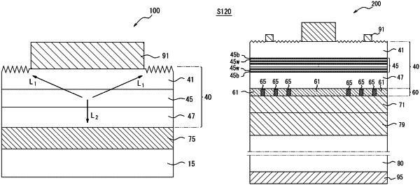
1. A semiconductor light-emitting element comprising:
a substrate;
a reflective layer on the substrate;
a first conductivity type cladding layer made of an InAsSbP-based III-V compound semiconductor containing at least In and As on the reflective layer;
an active layer with a center emission wavelength of 3400 nm or more and 4500 nm or less on the first conductivity type cladding layer; and
a second conductivity type cladding layer made of an InAsSbP-based III-V compound semiconductor containing at least In and As on the active layer,
wherein the second conductivity type cladding layer is on the light extraction side, and
an arithmetic average roughness Ra of a surface of a light extraction surface of the second conductivity type cladding layer is 0.07 μm or more and 0.7 μm or less, and a skewness Rsk of the surface is a positive value.
|