| CPC H01J 37/32082 (2013.01) [H01J 37/248 (2013.01); H01J 37/32568 (2013.01)] | 12 Claims |

|
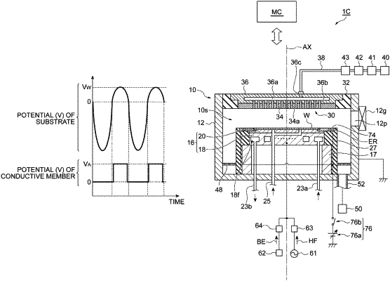
1. A plasma processing apparatus comprising:
a chamber;
a substrate support disposed in the chamber, the substrate support including:
a lower electrode; and
a conductive ring disposed closer to a side wall of the chamber than a substrate placed on the substrate support;
an RF power source configured to generate an RF power having a first frequency to generate a plasma in the chamber;
a bias power source configured to supply a bias to the lower electrode, the bias being a bias RF power having a second frequency less than the first frequency or a pulsed negative voltage which is periodically applied to the lower electrode at the second frequency, a waveform cycle of the bias defined by the second frequency including a first period in which a potential of the substrate is negative and a second period in which a potential of the substrate is equal to or greater than 0, the second frequency being not less than 50 kHz and not more than 27 MHz;
a power source device configured to apply a voltage to the conductive ring; and
a controller configured to control the power source device to apply a first voltage to the conductive ring in the first period in the waveform cycle and to apply a second voltage greater than the first voltage to the conductive ring in the second period in the waveform cycle, the second voltage having a positive polarity.
|