| CPC G11C 7/065 (2013.01) [G11C 11/417 (2013.01)] | 17 Claims |

|
1. A determination circuit comprising:
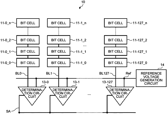
a differential pair included in a differential type determination circuit, one input terminal of the differential pair receiving a voltage of a bit line of a memory and another input terminal of the differential pair receiving a reference voltage; and
a first capacitive element that has one end connected to the other input terminal of the differential pair and another end receiving a determination circuit enable signal, the first capacitive element shifting, based on the determination circuit enable signal, a potential of the other input terminal so as to reduce a potential fluctuation of the other input terminal that occurs due to start of operation of the differential pair so that a difference between the voltage of the bit line and the reference voltage does not become small.
|