| CPC G11C 7/062 (2013.01) [G11C 11/16 (2013.01); G11C 13/004 (2013.01)] | 20 Claims |

|
1. A memory device, comprising:
a plurality of sense amplifiers;
a plurality of memory cells coupled to a plurality of first inputs of the plurality of sense amplifiers respectively;
a plurality of data lines coupled to a plurality of second inputs of the plurality of sense amplifiers respectively;
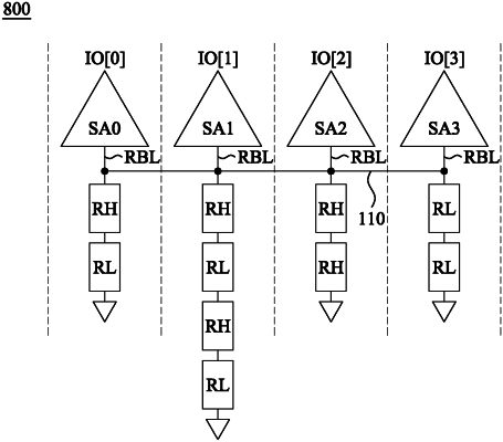
a plurality of reference cells arranged in a plurality of columns respectively and coupled to the plurality of data lines respectively, wherein the plurality of reference cells comprises a plurality of resistive elements,
wherein a first number of the resistive elements that have a first resistance and are ones, in the plurality of columns, closest to the plurality of sense amplifiers is different from a second number of the resistive elements that have a second resistance and are ones, in the plurality of columns, closest to the plurality of sense amplifiers, the first and second resistances being different from each other; and
a connection line coupled to the plurality of data lines,
wherein in a read mode, one of the plurality of sense amplifiers is configured to access the plurality of resistive elements arranged in one of the plurality of columns.
|