| CPC G11C 29/38 (2013.01) [G11C 11/1673 (2013.01); G11C 11/1675 (2013.01)] | 20 Claims |

|
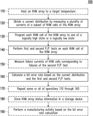
1. A method of testing a non-volatile memory (NVM) array, the method comprising:
heating the NVM array to a target temperature;
while the NVM array is heated to the target temperature:
programming a subset of NVM cells of the NVM array to first resistance levels and obtaining a first current distribution;
programming the subset of NVM cells to second resistance levels and obtaining a second current distribution;
calculating a current threshold level from the first and second current distributions; and
for each NVM cell of the NVM array:
programing the NVM cell to one of the first or second resistance levels; and
using the current threshold level to determine a first pass/fail (P/F) status and a second P/F status at the programmed resistance level; and
calculating a bit error rate (BER) of the NVM array based on the first and second current distributions and the first and second P/F status of each NVM cell of the NVM array.
|