| CPC G03G 15/065 (2013.01) [G03G 15/0806 (2013.01); G03G 15/0808 (2013.01); G03G 15/0266 (2013.01); G03G 15/04036 (2013.01); G03G 15/0865 (2013.01); G03G 15/2092 (2013.01); G03G 15/5004 (2013.01); G03G 21/0011 (2013.01); G03G 21/02 (2013.01); G03G 2215/0617 (2013.01)] | 4 Claims |

|
1. An image forming apparatus, comprising:
an image carrying member including a photosensitive layer formed on a surface thereof;
a charging device that charges the image carrying member to a prescribed surface potential;
an exposure device that exposes light to the surface of the image carrying member charged by the charging device so as to form thereon an electrostatic latent image with attenuated electrostatic charge;
a developing device including:
a development container for containing a non-magnetic one-component developer composed only of a toner;
a developer carrying member that is brought into pressure contact at a prescribed pressing force with the image carrying member and has an outer circumferential surface on which the toner is carried to form a toner layer;
a toner supply member that is brought into pressure contact at a prescribed pressing force with the developer carrying member and supplies the toner to the developer carrying member; and
a regulation blade that contacts the outer circumferential surface of the developer carrying member so as to regulate a thickness of the toner layer formed on the outer circumferential surface of the developer carrying member,
the developing device supplying the toner to the image carrying member on which the electrostatic latent image is formed;
a development voltage power supply that applies a development voltage Vdc to the developer carrying member and a supply voltage Vsdc to the toner supply member; and
a control section that controls the development voltage power supply,
wherein
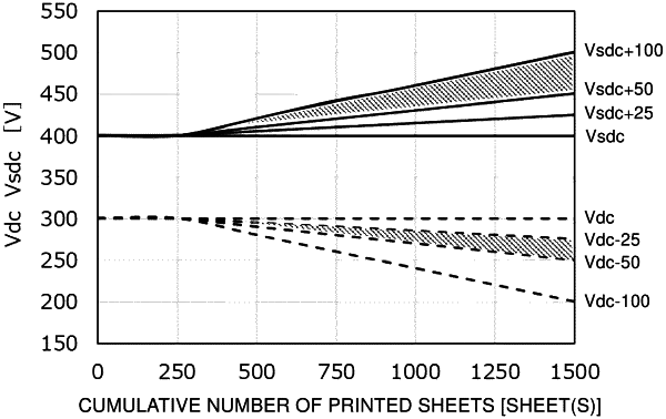
the control section performs control so that, as a cumulative drive time of the developing device from a start of use of the developing device increases, the supply voltage Vsdc becomes larger than a reference supply voltage and the development voltage Vdc becomes smaller than a reference development voltage, thus executing control to vary the development voltage Vdc and the supply voltage Vsdc so as to increase a potential difference Vsdc−Vdc between the supply voltage Vsdc and the development voltage Vdc.
|