| CPC G02F 1/167 (2013.01) [G02F 1/136209 (2013.01); G02F 1/136286 (2013.01); G02F 1/13718 (2013.01); G02F 1/1391 (2013.01)] | 10 Claims |

|
1. An electronic paper display screen, comprising a first electronic paper screen and a second liquid crystal display layer which are stacked, wherein
the first electronic paper screen is an electrophoretic electronic paper screen and the second liquid crystal display layer is a cholesteric liquid crystal display screen, and the second liquid crystal display layer comprises a first substrate, a second substrate and a control drive circuit;
the first substrate and the second substrate are oppositely provided, a plurality of first electrodes arranged in a first direction are provided on a side of the first substrate facing the second substrate, and a plurality of second electrodes arranged in a second direction are provided on aside of the second substrate facing the first substrate;
the first substrate comprises a first base, a first metal layer provided on the first base, a first passivation layer provided on the first metal layer, and a first electrode layer provided on the first passivation layer;
the second substrate comprises a second base, a second metal layer provided on the second base, a second passivation layer provided on the second metal layer, and a second electrode layer provided on the second passivation layer;
the first metal layer comprises a plurality of first metal wires, the second metal layer comprises a plurality of second metal wires, the first electrode layer comprises the first electrodes, the second electrode layer comprises the second electrodes, the first metal wires are connected to the first electrodes through a third opening in the first passivation layer, and the second metal wires are connected to the second electrodes through a second opening in the second passivation layer;
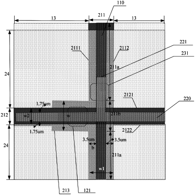
the first passivation layer is provided with at least one elongated first opening, the first metal wires are integrally overlapped with the first electrodes through the at least one first opening, and an orthographic projection of the first metal wires on the first base comprises an orthographic projection of the at least one first opening on the first base;
the second substrate further comprises a black matrix provided between the second base and the second metal layer, and an orthographic projection of the black matrix on the second base comprises an orthographic projection of the first metal wires on the second base and an orthographic projection of the second metal wires on the second substrate:
the black matrix comprises a plurality of first black matrices arranged along the first direction and a plurality of second black matrices arranged along the second direction, and a width of the first black matrix along the first direction is greater than a width of the second black matrix along the second direction;
the first black matrix comprises a first side and a second side oppositely provided along the first direction, a distance between an orthographic projection of the first side on the first base and an orthographic projection of the first metal wire adjacent to the first side on the first base is greater than or equal to a preset first distance, an orthographic projection of the second side on the first base coincides with an orthographic projection of a boundary of the first electrode adjacent to the second side close to the second side on the first base; and
the second black matrix comprises a third side and a fourth side oppositely provided along the second direction, an orthographic projection of the third side on the first base coincides with an orthographic projection of a boundary of the second electrode adjacent to the third side close to the third side on the first base, and an orthographic projection of the fourth side on the first base coincides with an orthographic projection of a boundary of the second electrode adjacent to the fourth side close to the fourth side on the first base.
|